Shenzhen Bicheng Electronics Technology Co., Ltd
深圳市碧澄电子科技有限公司
+86-755-27374946
info@bicheng-enterprise.com
WELCOME TO BICHENG


12-layer 1.6mm IT-180 Through Holes PCB--The Innovative Core with Thermal Stability and CAF Resistance

Shipped: 21st-JAN-2025

1. IT-180ATC Introduction

IT-180ATC is an advanced multifunctional filled epoxy that boasts a high glass transition temperature (175℃ as measured by DSC). It exhibits high thermal reliability and excellent resistance to CAF. This remarkable material is suitable for a wide range of applications and is capable of withstanding 260℃ lead-free assembly processes.


2. Features of IT-180ATC:

- Dielectric Constant of DK 4.1 at 10GHz

- Dissipation Factor of 0.017 at 10GHz

- Thermal resistance, T260 >60 minutes, T288 >20 minutes.

- Peel strength (Min.) Standard ED Copper, 8 lbs/inch

- CTE matched to copper with X axis of 11-13ppm/°C, Y of 13-15ppm/°C

- Low Z-axis coefficient of thermal expansion at 45 ppm/°C

- Tg >175 °C

- Low Moisture Absorption of 0.1%

- UL 94-V0 flammability rating.


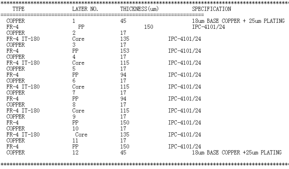
3. Basic PCB Specifications

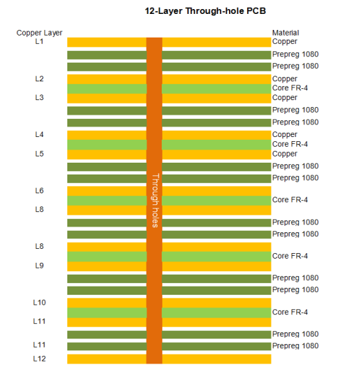
Board type: 12 layers

Material type: IT-180A, FR-4 Tg170 'C

Solder mask: Both sides, Matt Red

Silkscreen print: Top side, white

Surface finish: ENIG

Total board thickness: 1.6mm +/- 10%

Board size: 80.15mm x 76.6mm=1 PCS

Minimum hole size: 0.2mm

Solder mask thickness: 10um

Minimum dielectric thickness: 100um

Minimum trace line width: 120um

Minimum spacing: 125um

Plated through holes:L1-L12

Blind via: no

Impedance controlled:

50 ohm, differential pairs, Top layer, 4mil / 4 mil trace/gap, reference layer 2

90 ohm, differential paris, top layer, 5mil / 6 mil trace/gap, reference layer 2

100 ohm, differential paris, top layer, 6mil / 9 mil trace/gap, reference layer 2

50 ohm, differential pairs, layer 3, 5mil / 5 mil trace/gap, reference layer 2, layer 4

90 ohm, differential paris, layer 5, 7mil / 6 mil trace/gap, reference layer 4, layer 6

100 ohm, differential paris, layer 8, 6mil / 6 mil trace/gap, reference layer 7, layer 9

 
All vias with diameters of 0.2mm and 0.3mm are filled and capped in accordance with IPC 4761 Type VII. The printing of the series number is mandatory.
 
4. PCB Stack-up (Component side at top):


5. PCB Statistics:

Components: 240

Total Pads: 482

Thru Hole Pads: 234

Top SMT Pads: 138

Bottom SMT Pads: 110

Vias: 256

Nets: 10


6. Type of artwork supplied: Gerber RS-274-X
 
7. Quality standard: IPC-Class-2
 
8. Availability: worldwide

9. Some Typical Applications:
- Automotive (Engine room ECU)

- Backplanes

- Data Storage

- Server and Networking

- Telecommunications


NEXT: 2-layer 20mil CuClad250 PCB with a High PTFE Ratio, Leading the New Trend in Circuits


About Us
Products
Solutions
Contact Us


Antenna, Mobile Internet
Address:
6-11C Shidai Jingyuan, Fuyong, Baoan, Shenzhen, Guangdong, China 518103


Wireless Infrastructure
Phone:
86-755-27374946


Millimeter Wave Radar
Email:
info@bicheng-enterprise.com


Aerospace
 
WeChat:
bichengpcb


Satellite Navigation
 
Skype:
vickyxie0315@outlook.com


Power Amplifier


IoT


in fb yt quora


Copyright  © Shenzhen Bicheng Electronics Technology Co., Ltd. All rights reserved